High resolution Lcd Display Module,Tft Lcd Screen Display,Display Lcd Enclosure,Tft Display Lvds ESEN Optoelectronics Technology Co., Ltd, , https://www.esenoptoelectronics.com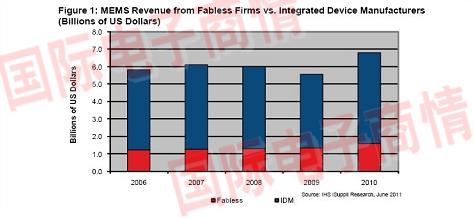 According to a study by IHS iSuppli Corporation, in 2010, fabless semiconductor companies expanded their share in the global micro-electromechanical systems (MEMS) market and last year accounted for nearly a quarter of total MEMS operating revenue.
In 2010, fabless semiconductor companies accounted for 23.2% of the total MEMS operating revenue, up from 21.3% four years ago. Although this four-year increase is not large, it shows that the MEMS manufacturing business is no longer monopolized by integrated device manufacturers (IDM) and continues to flow to other vendors. IDM designs and manufactures products internally. In contrast, fabless semiconductor companies, as their name suggests, do not have their own factories, but outsource their manufacturing operations to other specialized manufacturers, foundries.
The figure above shows the MEMS operating revenues of IDM and fabless semiconductor companies from 2006 to 2010.
The most important MEMS device inkjet printhead produced by the fabless semiconductor company accounted for 43% of the waferless manufacturing semiconductor company's MEMS operating revenue in 2010, the largest share, but lower than the 63% in 2006. In this area, Hewlett-Packard outsourced more than half of the print head wafers to STMicroelectronics, and Texas Instruments produced all the printheads entirely from Lexmark International. In addition, the fabless semiconductor company is an unknown printhead manufacturer in mainland China, and cooperates with MEMS foundries such as APM in Taiwan.
The second largest share of waferless manufacturing semiconductor MEMS operating revenue is MEMS pressure sensors, of which nearly one third outsourced manufacturing. For example, in the automotive sector, Sensata, Kavlico, and Melexis partner with various foundries such as SMI, GE, Micralyne, and X-Fab. As for industrial and medical applications, many manufacturers buy dies from foundries and then specialize in packaging.
In third place is MEMS microphones, and fabless semiconductor companies account for 99% of the market. Knowles Electronics is the industry leader, accounting for 85% of the MEMS microphone market, outsourcing all MEMS wafer manufacturing to Sony Kyushu. At the same time, Asiadino outsourced its business to TSMC, and Akustica outsourced MEMS microphones to Seiko Epson.
Optical MEMS is the fourth largest fabless semiconductor MEMS device. It accounts for a large proportion of the operating revenues of professional MEMS foundries such as Micralyne, Dalsa, IMT, and Memscap. These manufacturers have MEMS chip intellectual property rights. Optical MEMS also account for a large proportion of Colibrys’ operating revenue. According to general accounting principles, there are only two IDM vendors in the optical MEMS field - Dicon and Sercalo.
Gyro ranks fifth in fabless manufacturing semiconductor MEMS revenue, and InvenSense has achieved great success in consumer electronics. InvenSense outsourced 2-axis gyroscopes to Dalsa and outsourced 3-axis gyroscopes to Seiko Epson, TSMC and tMt. InvenSense accounted for 97% of the total fabless-free semiconductor gyroscope revenue last year, with the remaining share coming from military and aerospace applications, such as via French foundry Tronics, or from automotive applications through Melexis and foundry partner X-Fab.
Subdivision by Application, Largest Fabless Manufacturing Semiconductor Market 2010 The main application for semiconductorless MEMS is data processing, including inkjet print heads, hard disk timers, and scanning mirrors used in laser printers.
The second largest fabless semiconductor MEMS application is mobile and consumer electronics, and it is also the fastest growing application. Fabless manufacturing semiconductor microphones, gyroscopes and accelerometers are all important components in this field. Automotive is the third largest fabless semiconductor MEMS application, including pressure sensors, microbolometers, thermopiles, and gas sensors.
In terms of size from big to small, other major waferless manufacturing semiconductor MEMS application markets in 2010 included wireline communications, industrial, medical, civilian, and military aviation.
The fabless manufacturing semiconductor MEMS market will continue to grow IHS's forecast that the next five years will continue to grow without wafer semiconductor manufacturing MEMS business, mainly due to a variety of factors conducive to the market.
First, fabless semiconductor startups have introduced more innovative MEMS products that will enter the market. InvenSense is the most successful MEMS startup, but potential hot applications from other vendors are also under development. Among them are SiTime, Discera and Sand9 in the field of timers; Debiotech and CardioMEMS in the healthcare or biotech sector; Microstaq in the industrial and construction control sector.
Second, in the face of pressure from shareholders to maintain high profit margins, IDM and vertically integrated manufacturers may outsource some or all of their MEMS manufacturing operations to fabless semiconductor companies. In fact, several automotive systems companies that traditionally own their own factories, such as Delphi or Continental, have begun or will transition to fabless manufacturing semiconductor manufacturing.
Other factors that will promote the growth of fabless semiconductor MEMS business include the rejuvenation of optical MEMS in telecommunications, optical MEMS as the main source of revenue for various MEMS foundries, and the increasing content of MEMS in mobile phones and tablets. Wireless semiconductor companies have taken note of this trend, but they are not specialized in the MEMS field and will therefore need to align themselves with fabless semiconductor companies to get a slice of it and possibly increase wafer sales.
In order to realize a large-area high-resolution Liquid Crystal Display, it is usually necessary to use low-impedance metal materials, high-performance switching elements, and high-precision processing techniques. Aluminum is the most researched and used material for making TFT buses with low-impedance metals. By solving the problems of easy formation of hillocks, chemical corrosion and oxidation of aluminum, alloy methods (such as Al-Cu, Al-Si, Al-Nd and Al-Ti, etc.) and interlayer methods (such as Mo/Al/Mo) have been reported successively. , Cr/Al/Cr and Ti/Al/Ti, etc.), the alloy method is relatively simple in process, but the material has a higher resistivity. In May 1998, IBM developed a 16.3-inch ultra-high resolution (200ppi) a-Si TFT Display using Al-Nd alloy as the gate electrode, and mass production has been achieved. In April 1999, Toshiba introduced the 20.8-inch 16-SVGA (3, 200 × 2, 400) a-Si TFT-LCD, which can be said to represent the highest level of a-Si TFT-LCD in terms of high resolution and high capacity. .
According to Display Search in the third quarter of 2011, the global flat panel display research report "QuarterlyWorldw ide Flat Pane l Dis play Fore cas t Re port" pointed out that the average pixels per inch (ppi) in large-size LCD panels (>9.1 inches) ) Will grow from 88ppi in 2010 to 98ppi in 2015. The ppi of small and medium-sized LCD panels (<9.0 inches) will grow from 180ppi to 300ppi in the same period. With the rise of smart phones, mobile phones will be the most obvious application product for ppi's growth.
Another important way to realize high-resolution liquid crystal display is to develop LT p-Si TFT technology. The resolution of published p-SiTFT-LCD products is generally around 200ppi. Compared with a-Si TFT-LCD, LT p-Si TFT-LCD has a smaller volume of thin film transistors and storage capacitors. Therefore, it has a larger penetration area per inch, resulting in a brighter display. , And save more power. When the market demands higher ppi, low-temperature polysilicon (LTPS) technology becomes the best choice for manufacturing high-resolution thin-film transistor liquid crystal displays.
Contrast
The control ICs, filters and oriented films used in LCD manufacturing are related to the contrast of the panel. For general users, a contrast ratio of 350:1 is sufficient, but such contrast in the professional field does not satisfy users. Demand. Compared with CRT monitors easily reaching 500:1 or even higher contrast, only high-end LCD monitors can achieve this level. The first-tier LCD monitors on the market, such as Samsung, Asus, LG, etc., can reach a contrast ratio of 1000:1. However, because the contrast is difficult to accurately measure with instruments, you have to go and see it yourself when you pick it.
Tip: Contrast is very important. It can be said that the selection of LCD is a more important indicator than bright spots. When you understand that your customers buy LCDs for entertainment and watching DVDs, you can emphasize that contrast is more important than no dead pixels. We When watching streaming media, the brightness of the source is generally not large, but to see the contrast of light and dark in the scene of the character, the texture change from gray to black hair must be shown by the level of contrast. The 256-level grayscale in the test software In the test, more small gray grids can be seen clearly when looking up, which means that the contrast is better!a