First, the working principle speaker protection circuit shown in Figure 1. Mainly composed of midpoint potential detection circuit, delay circuit and relay. The circuit working process is: Twinkle System Technology Co Ltd , https://www.pickingbylight.com
At the moment when the audio power is turned on, since the voltage across the capacitor C3 cannot be abruptly changed, it can be regarded as a short circuit, and the potential of the 2nd and 6th pins of the time base circuit 555 is higher than 2/3 Vcc, so the 555 is in the reset state, and the 3-pin output is low. Level, transistor VT2 is off, relay JK normally open contact does not work. At the same time, the +12 V voltage is charged to the capacitor C3 through the resistor R4. After a delay of about 5 s (seconds), the potential of the 2 and 6 pins of the 555 is reduced to 1/3 Vcc, the 555 is triggered to be set, and the 3 pin is changed from the low level to the high level. Level, transistor VT2 is turned on, relay JK is energized, normally closed contact is closed, thus achieving a delay for a period of time to connect the speaker to the power amplifier, completely eliminating the impact of large current on the speaker when starting up.
When the audio power is turned off, the +12 voltage disappears quickly, but the output signal of the amplifier does not disappear immediately, and the impact noise generated by the shutdown process is also avoided.
When the power amplifier works abnormally or accidentally damages and the midpoint potential is too high (higher than 1.8 V), the DC voltage is limited by R1 and R2, and sent to C1, C2 filtering and D1~D4 rectification, about 1~2s (seconds). Transistor VT1 is turned on, 555's 4 pin is changed from high level to low level, 555 is directly reset, 3 pin output is low level, transistor VT2 is cut off, relay JK is de-energized, normally open contact is tripped, speaker is connected The amplifier circuit is disconnected, effectively protecting the speaker from damage.
By changing the parameters of R4 and C3, you can adjust the length of the delay time of the speaker protection circuit, which is usually set to 5 s (seconds). 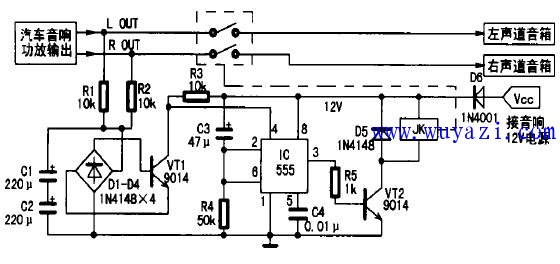
Second, component selection
The 555 must use a low-power CMOS time-base circuit. VT1 and VT2 use 9014 and C1815 low-power plastic-sealed transistors, which require a current amplification factor of β>100. D1 ~ D5 use 1N4148 type silicon switch diode, D6 is used for power supply reverse protection, 1N4001 ~ 1N4007 type silicon rectifier diode can be selected. R1 to R5 each use a 0.5 W five-color ring metal film resistor. C1, C2 use high-quality aluminum electrolytic capacitors, C3 should use tantalum electrolytic capacitor with small leakage and high precision, otherwise it will affect the delay precision. JK selects 12 V/7 A dual-type relay (one for each of the left and right channels), such as JZC-22F.