Further simplification, advanced digital power controller design
The challenge of isolating in digital power is how to quickly and accurately transmit digital or analog signals through isolated boundaries in a compact area. However, traditional optocoupler solutions have problems such as low bandwidth and large current transfer ratio (CTR) that varies greatly with temperature and time. The transformer solution has problems such as bulky size and magnetic saturation. These problems limit the use of optocouplers or transformers in certain high reliability applications, compact applications, and long life applications. This article discusses the use of digital isolation technology from Analog Devices' iCoupler® products to address these issues in digital power supply design.
Reasons for isolationWhen designing power supplies, adherence to safety standards is essential to protect operators and other personnel from electric shock and harmful energy. Isolation is an important method of meeting safety standards. Many global organizations (such as VDE and IEC in Europe and UL in the US) specify isolation requirements for different input and output voltage (steady state and transient) levels. For example, five insulating introduced in UL60950:
Functional insulation: Insulation required only during normal operation of the equipment.
Basic insulation: Provides insulation for basic electric shock protection.
Supplemental insulation: Independent insulation outside the basic insulation to reduce the risk of electric shock in the event of a basic insulation failure.
Double insulation: An insulation that includes basic insulation and supplementary insulation.
Reinforced insulation: A single insulation system that provides a degree of protection against electric shock and is equivalent to double insulation under the conditions specified in this standard.
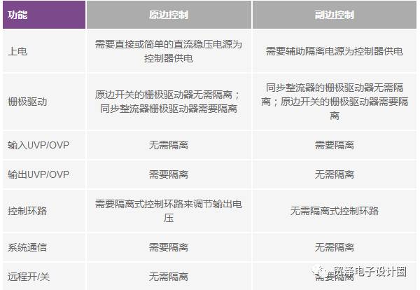
Primary side control and secondary side control comparisonAccording to the position of the controller, the isolated power control mode is divided into primary side control and secondary side control. Table 1 compares the functions of primary and secondary control. In the table below, UVP and OVP represent undervoltage protection and overvoltage protection, respectively.
Table 1. Comparison of primary and secondary control functions
 Secondary control
 The ADP1051 is ADI's advanced digital power controller with PMBusTM interface for high power density and high efficiency applications such as intermediate bus converters. Based on a flexible state machine architecture, the 2ADP1051 offers a number of attractive features such as reverse current protection, pre-bias startup, constant current mode, adjustable output voltage slew rate, adaptive dead time control, and volt-second balance. A large number of external components are reduced compared to analog solutions. In general, the ADP1051 is more commonly used for secondary side control because it is very convenient to communicate with the system. Therefore, the PWM signal of the synchronous rectifier and signals such as VOUT detection do not need to communicate with the system across the isolation boundary. In this case, however, the auxiliary power supply is required to supply initial power from the primary side to the secondary side controller ADP1051 during the startup phase. In addition, the PWM signal from the ADP1051 needs to cross the isolation boundary. Three solutions are discussed below, namely gate drive transformers, digital isolators, and isolated gate drivers.
Gate drive transformerFigure 1 shows a functional block diagram of a digital power supply using a gate drive transformer solution. In this solution, the secondary side controller ADP1051 sends a PWM signal to the ADP3654, which is a dual 4 A MOSFET driver. The ADP3654 then drives a gate drive transformer. The function of the gate drive transformer is to transfer the drive signal from the secondary side to the primary side and drive the primary MOSFET. The auxiliary isolated power supply supplies power to the ADP1051 during the startup phase.
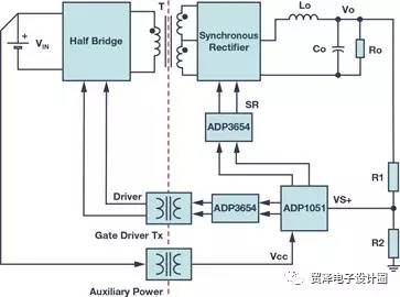 Figure 1. Driving the gate drive transformer with the ADP3654 solution.
 The advantages of gate drive transformer solutions include less latency and lower cost. But a more careful gate drive transformer design is needed because the transformer needs to be reset every time it passes, otherwise it will saturate. For gate drive transformer designs with half-bridge topologies, double-ended transformers are often used, as shown in Figure 2.
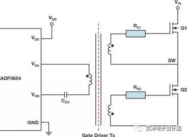 Figure 2. Double-ended gate drive transformer.
 Figure 2 shows the circuit of a gate drive transformer driven by the ADP3654. The VOA output and VOB output of the ADP3654 are connected to the gate drive transformer through a DC blocking capacitor CDC. The maximum 50% duty cycle is selected for the half bridge considering the maximum number of volts required for all operating conditions. After selecting the core, you can calculate the number of primary winding NPs using Equation 1 below:

Where VDD is the voltage across the primary winding, fs is the switching frequency, ∆B is the peak-to-peak flux density change over half of the switching period, and Ae is the equivalent cross-sectional area of ​​the core. When VOA is driven high and VOB is driven low, Q1 turns on and Q2 turns off. When VOB is driven high and VOA is driven low, Q2 turns on and Q1 turns off. It should be noted that this gate drive transformer is suitable for symmetrical half bridges and is not suitable for asymmetric half bridges or other active clamp topologies.
Digital isolatorFigure 3 shows a functional block diagram of a digital power supply implementing a digital isolator solution. The dual channel digital isolator, the ADuM3210, is used as a digital isolation to transfer the PWM signal from the secondary side controller ADP1051 to the primary half-bridge driver.
 Figure 3. Digital isolator solution.
 Compared to complex gate drive transformer designs, digital isolator solutions are smaller, more reliable, and easier to use. This solution has no duty cycle limitations and no saturation issues. High power density design is achieved due to more than 50% PCB space savings.
Isolated gate driverTo further simplify the design, the ADuM7223, a 4A isolated half-bridge gate driver with integrated electrical isolation and robust gate drive, provides independent isolated high-side and low-side outputs. Figure 4 shows an isolated gate driver solution.
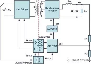 Figure 4. Isolated gate driver solution.
 In Figure 5, the ADuM7223 isolated gate driver is configured as a bootstrap gate driver to drive the half bridge. DBST is an external bootstrap diode and CBST is an external bootstrap capacitor. During each cycle of low-side MOSFET Q2 turn-on, VDD charges the bootstrap capacitor through the bootstrap diode. To minimize power consumption, ultrafast diodes with reduced forward voltage and short reverse recovery time are required.
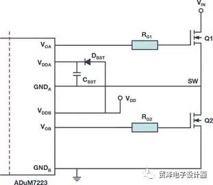 Figure 5. The isolated gate driver is configured as a bootstrap gate driver. Primary control
 Primary side control is more common in some low-cost applications because primary side control does not require an auxiliary isolated power supply and has a simple control architecture. Based on the isolated control path, three solutions are discussed below: linear optocouplers, common optocouplers (with standard amplifiers), and isolated amplifiers.
Linear optocouplerIsolate the output voltage in a digital power supply often requires fast and accurate isolation feedback. Optocouplers are often used to send analog signals from the secondary side to the primary side, but their CTR can vary greatly with temperature and performance will degrade over time. Figure 6 shows the normalized CTR and ambient temperature characteristics of TCET1100. In this figure, the rate of change of CTR will exceed 30% in the range of -25 ° C to +75 ° C.
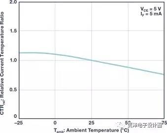 Figure 6. Normalized CTR and temperature for TECT1100.
 If a normal optocoupler is used directly in the feedback loop to transmit the output voltage, it is difficult to guarantee the output voltage accuracy. A common optocoupler, used in conjunction with an error amplifier, typically transmits a compensation signal instead of an output voltage signal. The ADP1051 has implemented digital loop compensation inside the chip, so no compensation signal is needed. One solution is to use a linear optocoupler to linearly transmit the output voltage, as shown in Figure 7. But linear optocouplers are costly, which means users have to pay extra.
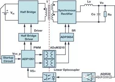 Figure 7. Linear optocoupler solution. Ordinary optocoupler (with standard amplifier)
 Alternatively, a normal optocoupler and a standard amplifier can be used to implement the primary side control circuit, as shown in Figure 8. In this example, high output voltage accuracy can be achieved without significant changes due to changes in the CTR temperature of the optocoupler. The measurement results show that the output voltage varies by ±1% when the CTR range is 100%-200%.
 Figure 8. Optocoupler (with amplifier) ​​solution.
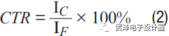
 The CTR formula is as follows
When the CTR changes with temperature, the output of the amplifier will compensate for this change to maintain the high accuracy of the output voltage. It should be noted that the stable operating point and swing range of the amplifier should be designed to meet the CTR temperature variation requirements to prevent the output of the amplifier from saturating.
Isolated amplifierThe third solution is an isolated amplifier, such as the ADuM3190 shown in Figure 9. The ADuM3190 is an isolated amplifier with high bandwidth and high accuracy compared to optocouplers, making it ideal for linear feedback supplies with primary side controllers. This solution offers improved transient response, power density and stability compared to popular optocoupler and shunt regulator solutions. The ADuM3190 achieves ±1% output voltage accuracy as long as it is properly designed.
 Figure 9. Isolated amplifier solution. Conclusion
 Today, isolation technology will play an increasingly important role due to the increasing security, high reliability, high power density, and intelligent management requirements of telecom, network, and computer power systems. Compared to traditional optocoupler and transformer solutions, Analog Devices' iCoupler ADuM3210, ADuM7223, and ADuM3190 combined with the digital power controller ADP1051 provide high reliability, high bandwidth, and high power density solutions.
Reference circuit
1 Baoxing Chen. “Micro-transformer isolation is beneficial for digital control.†Power Electronics Technology, October 2008.
2 ADP1051 data sheet. Analog Devices, 2014.
Author
Jason Duan
In 2000 and 2003, he obtained a bachelor's degree and a master's degree in electrical engineering from Xi'an Jiaotong University. He joined Analog Devices' power management division in Shanghai in 2007. In 2013, he moved from the Shanghai office to the San Jose office as a senior application engineer. He currently focuses on power electronics, including the development of advanced digital power controllers, ultra-low noise linear regulators and multi-channel PMU products.
Pharmaceuticals,2-Methyl- Propanoic Acid Monohydrate Price,2-Methyl- Propanoic Acid Monohydrate Free Sample,Pure 2-Methyl- Propanoic Acid Monohydrate
Zhejiang Wild Wind Pharmaceutical Co., Ltd. , https://www.wild-windchem.com