Circuit principle: The circuit of the automatic charger is shown in the figure below. The charger is mainly composed of RS trigger, charging voltage upper and lower limit setting circuit and power supply circuit. The RS flip-flop is composed of the 555 time base circuit A. The reference voltage of the two internal comparators is provided by the external voltage regulator VS of the 5-pin, so the reset level of the circuit is the voltage regulation value of VS, that is, 3V. The charging voltage upper limit setting circuit is composed of a potentiometer RP2 and a resistor R3; the charging voltage lower limit setting circuit is composed of a potentiometer RP3 and a resistor R4. The circuit power is supplied by the transformer T step-down, the diode VD1~VD4 bridge rectifier and the capacitor C1 filter. Spread Spectrum Communication System,Spread Spectrum Communication,All-outdoor Packet Radio,Outdoor Mobile Cell-sites Chengdu Zysen Technology Co., Ltd. , https://www.zysenmw.com
When charging, according to the number of sections of the battery G to be charged and the type of battery, adjust RP3 to set the lower limit voltage of charging, and adjust the upper limit voltage of RP2 to set the charging. Thus, when the battery G voltage is insufficient, the RP3 sliding terminal base circuit 2 pin level is less than V5/2 (here, V5 refers to the level of the time base circuit 5 pin, that is, the VS voltage regulation value is 3V), the time base circuit A is set, and the 3-pin output high level is charged to G by RP1 and VD5, and the VL is illuminated. When the G power is sufficient, the RP3's sliding terminal base circuit 6 pin level is greater than V5, the time base circuit is reset, the 3 pin output is low level, the charging is stopped, and the VL is extinguished. Adjusting the RP1 can adjust the charging current of the battery G, which should be determined according to the nature of the battery to be charged. For example, if the charging is normal, the charging current can be adjusted to about 50 mA. The function of the diode VD5 is to prevent the battery G from sinking current to the time base circuit after the charging is stopped. 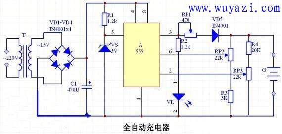
2. The automatic charger can charge 4 No. 5 nickel-cadmium batteries at a time. After the battery is fully charged, the circuit can automatically stop charging.
Circuit principle: The circuit of the automatic nickel-cadmium battery charger is shown in the figure below. The charger is mainly composed of power supply circuit, voltage comparator and indicating circuit. The circuit power supply is stepped down by transformer T, diode VD1~VD4 rectification, three-terminal voltage regulator integrated block A1 voltage regulator and capacitor C1, C2 filter supply. After the circuit is energized, it can output stable 9V DC voltage for charger. The voltage comparator consists of a time base circuit A2. A Zener diode VS (stabilized voltage 5.6V) is connected to the 5 terminal of its control terminal, so the reset level of the circuit is positioned at 5.6V. The light emitting diode VL is a charging indicator. The normal working voltage of the No. 5 nickel-cadmium battery is 1.2V, and the charging termination voltage is about 1.4V. G is a 4-cell nickel-cadmium battery to be charged, so the charge termination voltage is 4×1.4V=5.6V. After charging the battery into the charging stand, close the power switch S to start charging. Since the voltage across the capacitor C3 cannot be abruptly changed, when the power is turned on, the 2 pin of A2 is low level, A2 is triggered to be set, and the 3 pin outputs high level. This high level charges the battery G via the potentiometer RP and the diode VD5. Change the RP value to adjust the charging current. At this time, the 7 feet of A2 are suspended, and the VL illumination indicates that the circuit is charging. As the charging continues, the voltage across the G gradually rises. When it rises to 5.6V, A2 resets, the 3 pin outputs a low level, the charging automatically terminates, and the A2 internal discharge tube is turned on, and the 7-pin output is low. VL off indicates the end of charging. 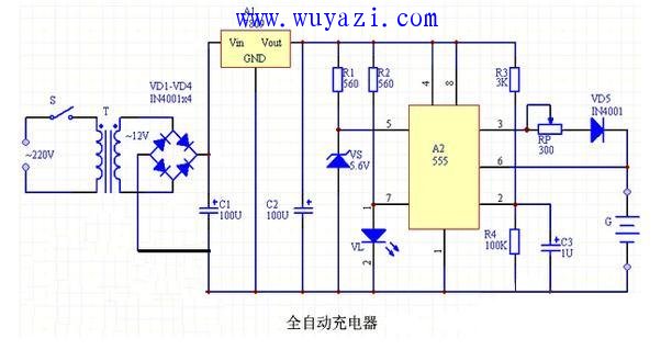
Review analysis:
In the first figure, VD1~VD5 selects silicon rectifier diodes such as IN4001. VS selects 3V, 1/2W Zener diode. VL uses ordinary red LEDs. RP selects 2W wirewound potentiometer; RP2, RP3 selects ordinary small synthetic carbon film potentiometer, such as WH5 type; R1~R4 selects 1/8W carbon film resistor. C1 selects CD11-25V aluminum electrolytic capacitor. T selects 220V/15V, 5VA small high quality power transformer. 4 section 5 nickel-cadmium batteries are charged. The second picture A1 selects the LM7809 three-terminal regulator integrated block, which should be equipped with an aluminum heat sink. VD1~VD5 selects IN4001 type silicon rectifier diode. VS selects 5.6V, 1/2W Zener diodes, such as UZ-5.6B, IN5232 type. VL uses ordinary red LEDs. RP selects 2W wirewound potentiometer, R1~R4 select 1/8W carbon membrane resistor for use. C1 selects CD11-25V aluminum electrolytic capacitor, C2 and C3 are CD11-16V aluminum electrolytic capacitor. S selects the ordinary 1×1 power supply small switch. T selects 220V/12V, 5VA small high quality power transformer.