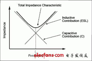
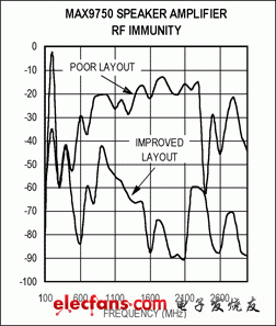
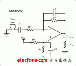
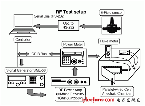
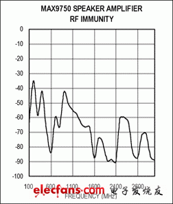
introduction RF suppression is also known as RF sensitivity. It has become an important design element of PSRR, THD + N and SNR in the audio field of mobile phones, MP3 players and notebook computers. Bluetooth technology is gradually being applied to mobile devices as a wireless serial cable replacement for headsets and microphones. The wireless local area network (WLAN) technology using IEEE 802.11b / g protocol has also become the standard configuration of personal computers and notebook computers. TDMA multiplexing in GSM, PCS and DECT technologies will introduce greater RF interference. Today's dense RF environment has triggered industry attention to the RF sensitivity of electronic circuits and the impact of RF on overall system integrity. The audio amplifier is a system module sensitive to RF. The audio amplifier will demodulate the RF carrier and reproduce the modulated signal and its harmonic components at its output. Some frequencies will fall into the range of the audio baseband, thus creating a "buzzing" sound that the user does not want to hear at the speaker output of the system. To avoid this problem, the system designer must fully understand the limitations of the selected amplifier IC and its corresponding PCB layout. This article will guide the designer how to optimize the RF suppression capability of the audio amplifier circuit board. Find the source of RF noise The key to a good layout (ie, good RF suppression) is to first identify the source of RF coupling noise. If the selected audio amplifier has an evaluation board, you can use the evaluation board to check the RF sensitivity of each pin. Choose a frequency of interest, such as 2.4GHz in WLAN applications. According to the antenna principle, an antenna with a lead length of 1.2 inches (a quarter wavelength of a 2.4 GHz RF signal) is very efficient at a frequency of 2.4 GHz. l = c / (4 * f) Where l = length, c = 3X10⁸, and f = frequency. Take a 1.2-inch wire and solder it directly to one pin of the IC, and measure (see appendix) the IC's RF suppression capability at the frequency of interest (2.4 GHz ± 10%). Remove the 1.2-inch lead and solder it to the other pin of the amplifier, and repeat the RF measurement process. Please ensure that the conditions of each test are consistent. Continue to measure in this way until the 1.2-inch wire is connected to each pin of the amplifier, and record the RF measurement results at the frequency of interest. Finally, without the antenna connected to the pin, measure the IC's RF suppression capability. The last test provided us with a benchmark of amplifier performance. Comparing this test result with previous test results, the amplifier pin most sensitive to the RF demodulated signal can be obtained. Using these data, we can optimize the PCB design to reduce the RF noise coupled to the amplifier pins. MAX9750 example analysis: The engineering evaluation results show that the nine pins with the highest RF sensitivity in the MAX9750 IC: INL, INR, BIAS, VOL, BEEP, OUTL_, and OUTR_. The role of capacitance Take the BIAS pin of the selected IC as an example. Assuming that the BIAS pin has poor RF suppression at the frequency of interest, the PCB design that should be considered first is to shorten the length of the lead from the BIAS pin to the decoupling capacitor. If the RF demodulation situation is not ideal after optimizing the lead length, consider adding a small bypass capacitor (approximately 10pF to 100pF) to the ground at the amplifier pin. The impedance characteristic of the capacitor can form a notch filter at the most sensitive frequency of the system (in this case, 2.4 GHz). Please refer to the impedance characteristics of the capacitance model (C1) in Figure 1A. Figure 1A. Non-ideal capacitance model Figure 1B. Non-ideal capacitance model, impedance characteristics If C1 is an ideal capacitor, the impedance characteristics will decrease with increasing frequency (XC = 1 / [2π xfx C]). However, there is no ideal capacitor in practical applications. The impedance of the non-ideal capacitance model (Figure 1B) sags at the self-resonant frequency * and then starts to rise with frequency. When the frequency is greater than fo, the inductance component begins to increase (XL = 2π xfx L). If the capacitor is used as a filter, when it is close to or higher than its self-resonant frequency, this characteristic will make the filtering effect worse. However, if the capacitor is selected to bypass a specific high-frequency component to ground, then the self-resonance characteristic of the capacitor can come in handy. MAX9750 example analysis: 33pF capacitor is added to the BIAS pin to improve the RF suppression capability (average 3.6dB). Control input pin noise Generally, the input pin of the audio amplifier is always the source of RF coupling noise, so make sure that the length of the input lead is less than 1/4 of the system's RF signal wavelength. The quiet ground plane also reduces RF noise coupled to the input pins. There should be a quiet ground layer around each input lead of the IC. This ground plane helps isolate the input pins of the selected audio amplifier from any high-frequency RF signals. MAX9750 example analysis: shortening the length of the input lead by three times and laying a ground layer on the left channel, right channel, and PC-beep pins will further improve the RF suppression capability of the MAX9750 IC (Figure 2). Figure 2. MAX9750C speaker amplifier RF suppression capability test results: noise floor = -94.4dBV. Note: Figure 2 shows the typical RF suppression capability of the MAX9750 IC. Some external factors such as antenna signal strength, cable length, and speaker type also affect RF suppression performance. We can also use some high-cost methods, such as adding LC filters to the pins of amplifiers with higher RF sensitivity or adding low ESR capacitors to the circuit board. These methods are effective, but the cost is higher. If the source of RF noise can be determined, there is no need to use a high-cost solution. to sum up Audio amplifiers with poor RF rejection can affect the integrity of the overall system design. If you can find the source of the problem, you can take appropriate measures to avoid audio RF demodulation. Normally, the input, output, bias, and power supply leads should be less than 1/4 of the system RF signal wavelength. If you need to improve RF suppression, you can use a small capacitor to directly ground the IC pin (even if a large capacitor is connected to this pin), and lay a ground layer near the sensitive amplifier pin. Finally, keep high-power RF system modules away from susceptible audio amplifier pins. After these measures are taken, the "nasty" audio demodulation "buzz" will be eliminated. * During self-resonance, capacitive and inductive impedances cancel each other out, leaving only resistive components. The self-resonant frequency is: appendix To obtain accurate and repeatable test results, we need to place the device under test (DUT) in an RF field of known strength. Maxim has developed a set of test methods: an RF shielded laboratory, a signal generator, an RF amplifier, and a field strength detector to measure RF sensitivity to obtain reliable and repeatable test results. Figure A. RF noise suppression capability measurement circuit Figure A above is a typical op-amp test setup (op-amp). The non-inverting input of the amplifier is shorted to ground through a 1.5-inch loop wire (analog PCB lead). We chose a standard 1.5-inch input lead, so that the RF suppression capabilities of multiple Maxim amplifiers can be compared (Note: The input lead from the DUT to the input source has an antenna effect in the system's sensitive frequency range). A predetermined load is connected to the output of the amplifier. Then, the amplifier is placed in a shielded test chamber. Maxim's RF shielding test system simulates an RF environment and monitors the demodulated signal at the output of the amplifier. Figure B. Maxim's RF suppression test method Figure B shows Maxim's RF shielding test system, which simulates the RF field environment required for RF suppression tests. The test cavity is similar to the shield room of the Faraday cavity, isolating the device under test from the external electric field. The complete test system contains the following equipment: Signal generator: SML-03, 9kHz to 3.3GHz (Rhode & Schwarz) RF power amplifier: 20MHz to 1000MHz, 20W (OPHIR 5124) RF power amplifier: 1GHz to 3GHz, 50W (OPHIR 5173) Power meter: 25MHz to 1GHz (Rhode & Schwarz) Parallel line unit (shield cavity) Field strength detector Computer (PC) Fluke digital multimeter (dBV meter) Use the computer to set the frequency range, modulation ratio and modulation type output by the signal generator, and the power output of the RF power amplifier. The modulated signal is fed to the corresponding power amplifier (OPHIR 5124: 20MHz to 1000MHz, 20W or OPHIR 5173: 1GHz to 3GHz, 50W), and the output of the amplifier is measured and monitored by the directional coupler and power meter. The defined RF field is radiated uniformly in the test chamber. During the test, Maxim placed the device under test in the center of the shielded room. The field strength detector continuously detects the 50V / m uniform field strength where the measured piece is located. The signal used is an RF sine wave with a frequency between 100MHz and 3GHz, modulated with an audio frequency of 1kHz, with a modulation degree of 100%. The test port is powered by the access port of the test room, and the output monitoring device is connected through the access port. Use a Fluke multimeter (in dBV units) to monitor the demodulated 1kHz signal amplitude in real time. When the RF sine wave frequency is changed between 100MHz and 3GHz according to the preset settings, the report result of the Fluke multimeter is recorded. Figure C is the test result of 100MHz to 3GHz frequency sweep. Figure C. MAX9750 RF suppression test results
P3.91-7.82 Transparent LED Display
Features:
*Ventilated light
* Nova MSD 300 sending card and Nova A5S receiving card
* High debugging brightness and no damage to gray scale, achieving the debugging technology for nice image.
* Passed the TÃœV,FCC,ROHS,CE cetification.
Our company have 13 years experience of led display and Stage Lights , our company mainly produce Indoor Rental LED Display, Outdoor Rental LED Display, Transparent LED Display,Indoor Fixed Indoor LED Display, Outdoor Fixed LED Display, Poster LED Display , Dance LED Display ... In additional, we also produce stage lights, such as beam lights Series, moving head lights Series, LED Par Light Series and son on...
Application:
Movie theaters, clubs, stages.
Transparent LED Display,Transparent Led Display,Transparent Poster Led Display,Led Screen Panel Guangzhou Chengwen Photoelectric Technology co.,ltd , https://www.cwleddisplay.com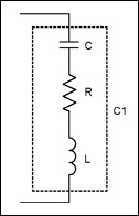
![]()
*Free air conditioning heat saving energy
*Environmental protection- it uses only a third of the power of a conventional Led screen
* Convenient installation High compatibility
Supermarket, large-scale shopping malls, star-rated hotels, travel agencies
* Financial Organizations:
Banks, insurance companies, post offices, hospital, schools
* Public Places:
Subway, airports, stations, parks, exhibition halls, stadiums, museums, commercial buildings, meeting rooms
* Entertainments:
Using PCB layout technology to realize RF noise suppression of audio amplifier
* Cabinet size:1000x500mm
* Kinglight/Nationstar LED Lamp, Refresh rate:1920-3840hz
* Ultra-Light designing, less than 6.5kg/pcs, hanging or floor mounted installation, no need the heavy steel structure.
* High brightness up to 3500cd/sq.m, even in the sunlight conditions can see clear, but low power consumption to save the electric power cost.