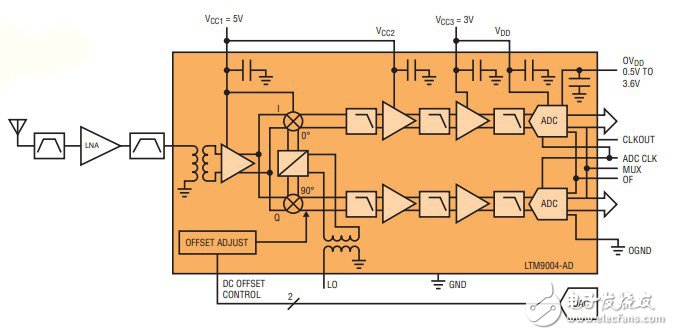
Under the premise of meeting the performance requirements of macrocell base stations, how high can the integration be? Process technology still limits that certain important functional components must be manufactured using special processes: GaAs and SiGe processes are used in the radio frequency (RF) field, fine-line CMOS processes are used for high-speed ADCs, and high-quality (High-Q) filters It is well realized using semiconductor materials. In addition, the market's demand for improved integration has not stopped. Considering the above issues, Linear Technology decided to use System-in-Package (SiP) technology to develop a receiver with a board area of ​​about 1/2 square inch (just over 3cm2). There are 50Ω RF input, 50Ω LO input, ADC clock input and digital ADC output at the receiver boundary. This boundary is reserved for the addition of low-noise amplifiers (LNA) and RF filtering for input, LO and clock generation, and digital processing of digital outputs. Within the 15mm x 22mm package is a signal link using SiGe high-frequency components, discrete passive filtering, and thin-line CMOS ADCs. This article will analyze and design the LTM® 9004 Micro Module (µModule®) receiver (a direct conversion receiver). Design goals The design goal is a Universal Mobile Telecommunications System (UMTS) uplink frequency division duplex (FDD) system, especially a medium coverage base station in the operating band I (see 3GPP TS25.104 V7.4.0 for details). For the receiver, sensitivity is a major consideration. When the input signal-to-noise ratio (SNR) is -19.8dB / 5MHz, the required sensitivity is ≤-111dBm. This means that the effective noise floor at the input of the receiver must be ≤-158.2dBm / Hz. Design analysis: Zero IF or direct conversion receiver LTM9004 is a direct conversion receiver using I / Q demodulator, baseband amplifier, and dual 14-bit 125Msps ADC (as shown in Figure 1). The LTM9004-AC low-pass filter has a 0.2dB corner at 9.42MHz, allowing 4 WCDMA carriers. The LTM9004 can be used with an RF front end to form a complete UMTS band uplink receiver. The RF front-end consists of a duplexer and one or more low-noise amplifiers (LNA) and ceramic band-pass filters. To minimize gain and phase imbalance, the baseband link uses a fixed-gain topology. Therefore, an RF variable gain amplifier (VGA) needs to be installed before the LTM9004. Here is a typical performance example of such a front end: Receive (Rx) frequency range: 1920MHz to 1980MHz RF gain: 15dB (maximum) Automatic Gain Control (AGC) Range: 20dB Noise figure: 1.6dB IIP2: + 50dBm IIP3: 0dBm P1dB: -9.5dBm Suppression at 20MHz: 2dB Transmit (Tx) frequency band suppression: 96dB Figure 1: Direct conversion architecture implemented in the LTM9004 micro-module receiver Considering the effective noise impact of the RF front end, the maximum allowable noise caused by the LTM9004 must be -142.2dBm / Hz. The typical input noise of the LTM9004 is -148.3dBm / Hz, and the system sensitivity calculated from this is -116.7dBm. Generally, such receivers can benefit from DSP filtering of some digitized signals after the ADC. In this case, assume that the DSP filter is a 64-tap RRC low-pass filter with α = 0.22. In order to work in the presence of co-channel interference signals, the receiver must have sufficient dynamic range at maximum sensitivity. The UMTS specification requires a maximum co-channel interference of -73dBm. Please note that for a modulated signal with a 10dB crest factor, the input level of -1dBFS is -15.1dBm within the IF passband of the LTM9004. At the input of the LTM9004, this is equivalent to a digitized signal level of -53dBm, or -2.6dBFS. When the RF automatic gain control (AGC) is set to the minimum gain, the receiver must be able to demodulate the maximum signal expected from the mobile phone. This requirement ultimately sets the maximum signal size that the LTM9004 must provide to -1dBFS or below. The minimum path loss required by the specification is 53dB, and the average power of the mobile phone is assumed to be + 28dBm. Then at the receiver input, the maximum signal level is -25dBm. This is equivalent to a peak value of -14.6dBFS. Several blocking signals are specified in the UMTS system specification. In the presence of such signals, only the specified size of desensitization is allowed, and the sensitivity index is -115dBm. The first of these is an adjacent channel 5 MHz apart, with a level of -42 dBm. The peak value of the digitized signal level is -11.6dBFS. DSP post-processing will increase the 51dB suppression, so this signal is equivalent to a -93dBm interference signal at the receiver input. The final sensitivity is -112.8dBm. Moreover, the receiver must also compete with an interference channel of -35dBm separated by ≥10MHz. The IF suppression of the μModule receiver will attenuate this interfering channel to a digital signal level equivalent to a peak value of -6.6dBFS. After DSP post-processing, it is equivalent to -89.5dBm on the input end of the receiver, and the final sensitivity is -109.2dBm. In addition, out-of-band blocking signals must also be considered, but the level of these out-of-band blocking signals is the same as the in-band blocking signals already discussed. In all these cases, the LTM9004's typical input level of -1dBFS is far above the maximum expected signal level. Please note that the crest factor of the modulated channel will be approximately 10dB ~ 12dB, so at the output of the LTM9004, the largest one will reach a peak power of about 6.5dBFS. The largest blocking signal is -15dBm continuous wave (CW) tone (≥20MHz beyond the edge of the receiving band). The RF front end will provide 37dB of suppression for this tone, so it will appear at -32dBm when it appears at the input of the LTM9004. At this time, this level of signal is still not allowed to reduce the sensitivity of the baseband μModule receiver. The peak value of the equivalent digital level is only -41.6dBFS, so it has no effect on sensitivity. Another unwanted source of interference signal power is leakage from the transmitter. Because this is an FDD application, the receiver described here will be coupled to a transmitter that works simultaneously. The output level of the transmitter is assumed to be ≤ + 38dBm, while the "send to receive" isolation is 95dB. Then, the leakage at the input of the LTM9004 is -31.5dBm, and the offset from the received signal is at least 130MHz. The equivalent peak value of the digitized level is only -76.6dBFS, so the sensitivity will not be reduced. One challenge of the direct conversion architecture is second-order linearity. Non-ideal second-order linearity will allow any desired or undesired signal to enter, which will cause DC offset or pseudo-random noise on the baseband. If this pseudo-random noise is close to the noise level of the receiver, then the blocking signals discussed in detail above will reduce the sensitivity. In all cases where these blocking signals exist, system specifications allow for sensitivity reduction. According to the system specification, -35dBm blocking channel can reduce the sensitivity to -105dBm. As we saw above, this blocking signal constitutes a -15dBm interference signal at the receiver input. The second-order distortion generated by the LTM9004 input is approximately 16dB lower than thermal noise. As a result, the predicted sensitivity is -116.6dBm. A -15dBm CW blocking signal will also cause a second-order component; in this case this component is a DC offset. DC offset is undesirable because it reduces the maximum signal that the A / D converter can handle. A reliable method to mitigate the effects of DC offset is to ensure that the second-order linearity of the baseband μModule receiver is sufficiently high. At the input of the ADC, the predicted DC offset due to this signal is <1mV. Please note that transmitter leakage is not included in the system specifications. Therefore, the decrease in sensitivity due to this signal must be kept to a minimum. The output level of the transmitter is assumed to be ≤ + 38dBm, while the "send to receive" isolation is 95dB. The sensitivity loss due to the second-order distortion generated in LTM9004 will be <0.1dB. There is only one requirement for third-order linearity in the specification. This is because in the presence of two interfering signals, the sensitivity must not fall below -115dBm. The two interfering signals are a CW tone and a WCDMA channel, and their sizes are both -48dBm. These interfering signals appear at the input of LTM9004 with a size of -28dBm. Their frequencies are separated from the desired channel by 10MHz and 20MHz, so the third-order intermodulation components will be located at baseband. At this time, this component still appears in the form of pseudo-random noise, thus reducing the signal-to-noise ratio. The third-order distortion generated in the LTM9004 is approximately 20dB lower than the thermal noise layer, and the expected sensitivity drop is <0.1dB. Football Stadium Advertising LED Screen
This series is a classic football field advertising LED Screen, which is specially used for advertising display in various stadiums, such as football fields, basketball courts, badminton courts, tennis courts, volleyball courts and other competitive sports halls. Football Stadium Advertising LED Screen with IP65 waterproof level, excellent anti-collision ability, can resist the impact of balls. High brightnesee makes good perfomance even under sunshine. Good protection design on top of cabinet with thick anti-collision cotton.
Football Stadium Advertising Led Screen,Led Panel Display,Led Video Panel, Football Cup Led Display Billboards Guangzhou Cheng Wen Photoelectric Technology Co., Ltd. , https://www.cwdisplay.com