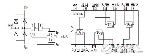
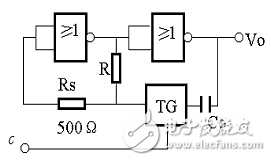
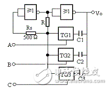
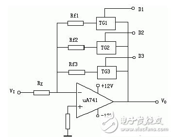
The so-called transmission gate (TG) is an analog switch that transmits analog signals. The CMOS transmission gate is formed by a P-channel and an N-channel enhancement MOS transistor in parallel, as shown in FIG. 1 . TP and TN are symmetrical devices whose drain and source are interchangeable. Let the input analog signal vary from -5V to +5V. In order to make the PN junction between the substrate and the drain source not to be positively biased at any time, the substrate of the TP is connected to the +5V voltage, and the substrate of the TN is connected to the -5V voltage. The gates of the two tubes are controlled by complementary signal voltages (+5V and -5V), respectively. (а) circuit (ь) symbol Figure 1 CMOS transmission gate The working conditions of the transmission gate are as follows: When c is connected to low level (-5V), the gate voltage of TN is -5V, uI is any value within the range of -5V to +5V, and TN is not conductive. At the same time, the gate voltage of TP is +5V, uI is anywhere from -5V to +5V, and TP is also non-conductive. It can be seen that when the c termination is low, the switch is open. To enable the switch, c can be connected high (+5V). At this time, the gate voltage of TN is +5V, uI is in the range of -5V to +3V, and TN is turned on. At the same time, the gate voltage of TP is -5V, and TP will be turned on when uI is in the range of -3V to +5V. From the above analysis, we can see that when uI<-3V, only TN is turned on, and when uI>+3V, only TP is turned on. When uI is in the range of -3V to +3V, both TN and TP are turned on. Further analysis can also see that the deeper one tube is conducting, the less conductive the other tube is. In other words, when the on-resistance of one tube decreases, the on-resistance of the other tube increases. Since the two tubes are operated in parallel, it can be approximated that the energy-conducting resistance of the switch is approximately a constant. This is the advantage of CMOS transmission gates. Figure 2 shows the logic diagram and external lead arrangement of the CC4016. (a) Logic diagram (b) Outer lead arrangement diagram Figure 2 Quadruple Bidirectional Switch CC4016 (1) Gated oscillator As shown in FIG. 3, when c is "1", the TG conduction circuit oscillates and VO outputs a square wave; when c is "O", TG is turned off and the circuit stops oscillating. Figure 3 gated oscillator (2) Programmable pulse oscillator If you want to obtain different frequency square wave can be used as shown in Figure 4, as long as the A, B, C by adding different levels of control, you can get a rectangular wave of different frequencies. Figure 4 programmable pulse oscillator (3) Programmable operational amplifier The transmission gate can transmit digital signals, and can also transmit analog signals. The feedback part of the operational amplifier adopts program control, which can change the amplifier's voltage amplification. Figure 5 programmable amplifier Figure 5 program-controlled amplifier Grid Fan ,Grid Ceiling Fan,Off Grid Ceiling Fan,Off Grid Fan Hangzhou Jinjiu Electric Appliance Co Ltd. , https://www.jinjiufanmotor.com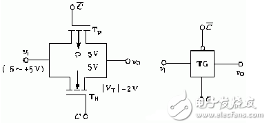
What are the cmos transmission gate chip models?
Transmission Gate Basics