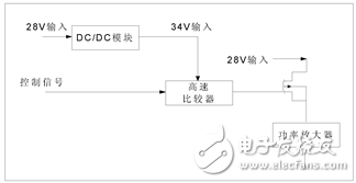
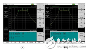
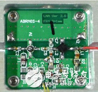
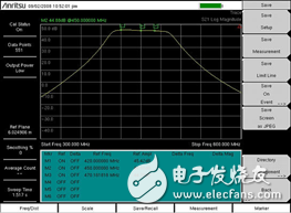
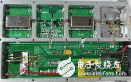
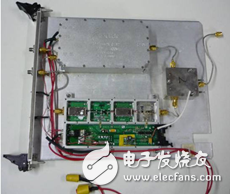
Transient polarization new system radar has extremely important military value in improving the detection performance and sensing ability of radar system in complex battlefield environment and in anti-jamming, anti-stealth and anti-low-altitude penetration. Its main function is to detect the polarization scattering characteristics of the radar target, and simultaneously measure the four parameters of the target's polarization scattering matrix, which avoids the inherent measurement accuracy of the traditional time-sharing polarization measurement system and the complexity of compensation and calibration. It provides a technical guarantee for accurately measuring the polarization scattering matrix of moving targets. The T/R component is an important part of the transient polarization radar RF system. It mainly performs functions such as transmit power amplification, transceiver isolation and receiving low noise amplification. As shown in Figure 1, the RF signal from the upconversion component is amplified by the power amplifier and output by the circulator to the antenna feeder system. The received signal is sent by the circulator to the limiter, via the receiver switch, filter and low noise. The amplifier is amplified and sent to the downconverter. This article will focus on the design process for power amplifier high-speed switching, limiter, receive switch, receive preselect filter, and low noise amplifier. Figure 1 Schematic diagram of T/R component structure 3 T/R component design 3.1 Power amplifier power supply high speed switch design During reception, the signal received by the antenna enters the receiving link through the circulator, and the noise and local oscillator signals amplified by the power amplifier are also coupled to the receiving link. In comparison, the noise coupled to the receiving channel and the local oscillator signal may be compared. The useful signal is so large that it floods the useful signal and even blocks the receiver. To solve this problem, the power of the power amplifier is turned off during reception. The control signal for cutting off the power amplifier is taken from the transceiving switching control signal. The retransmission of the system is higher, so the power amplifier power supply is also turned off and on at a higher speed. A field effect switch is used as a switch for the power amplifier power supply. 2 is a block diagram of a power amplifier power switch structure. The control signal (TTL level) is shaped by a high-speed comparator to a low level close to 0V, and a driving signal with a high level close to 34V is sent to the gate of the FET when the driving signal is At 0V, the FET is turned off and the power of the power amplifier is cut off. When the drive signal is 34V, the FET is turned on and the power of the power amplifier is turned on. Figure 2 Power amplifier power switch block diagram 3.2 Limiter design The limiter is often used in the front stage of the receiving device to limit the high-power input signal exceeding the threshold to protect the sensitive circuit and device of the latter stage. The limiter typically consists of a DC blocking capacitor on the input and output ports and an integrated diode limiter circuit. Integrated circuit contains 50 through 3.2 High-speed receiving switch design During the transmission of the transmitter, most of the energy output by the power amplifier is fed into the antenna through the circulator because the isolation between the two ports isolated by the circulator is about 25 dB, so there is still a small amount of energy coupled to the circulator to receive the output. Port, the antenna is not ideally matched, which causes the energy coupled to the circulator to receive the output port. This part of the energy is attenuated to the level of the rear circuit without being damaged by the limiter in front of the receiving channel, but the signal level after attenuation is still It is enough for the low-noise amplifier and other post-active circuits to enter the deep saturation state. It takes a certain time for the circuit to return from the deep saturation state to the normal working state. This time is called the saturation recovery time. The saturation recovery time increases the radar's blind distance. According to the design requirements, the transmission and isolation isolation during transmission needs to be greater than 90dB. When the circulator is well matched, the isolation between the isolated ports is 25 dB. Considering the slight mismatch of the antenna, the isolation of the circulator can only be considered as 20 dB. Therefore, the on/off ratio of the receiving switch should exceed 70 dB. Figure 3 Schematic diagram of ohmic impedance termination limiter The speed of the receiving switch affects the blind distance of the radar detection, so the high-speed RF switch should be selected as the receiving switch. ADG901 is selected as the switching component for making the receiving switch, and its input and output ports are connected 50 Figure 4 High-speed receiver switch and limiter 3.3 Receive preselected filter design In order to obtain a better receiver front end, filter out various interfering signals in the receiver, and retain the useful signal, the filter must be placed in the appropriate place at the front end of the receiver, especially the preselected filter placed in the first stage of the system. Its performance directly affects the noise figure of the RF front end of the entire receiver. The loss of the preselected filter must be minimized and must also have the selection characteristics required by the system. The actual selection is a class 1 ceramic capacitor filter. Figure 5 shows the test results of the dual-channel preselection filter. It can be seen that the out-of-band filtering characteristics are extremely steep and the suppression performance is good. The passband ripple is less than 0.3dB. And the stop band indicator meets the design requirements. Figure 5 Received preselected filter performance measured results 3.4 Low Noise Amplifier Design In various specific wireless communication systems (bandwidth BW, demodulation signal-to-noise ratio S/N), the key factor to effectively improve the sensitivity is to reduce the noise figure NF of the receiver, and the key to determine the noise figure of the receiver. The component is the low noise amplifier at the front end of the receiver. The main function of the low noise amplifier is to amplify the weak signal received by the antenna from the air and reduce the noise interference for the system to demodulate the required information data, so the design of the low noise amplifier is crucial for the entire receiver. . The low noise amplifier of this system adopts a two-stage series form, and has a sufficiently high gain while the noise figure satisfies the design specifications. The front stage uses Vantone's WHM02AE, and the latter stage uses Mini-circuits' MAR-8ASM. Since the WHM02AE uses only a small number of different peripheral components, it can form the lowest noise figure and the best match, and is suitable for amplifiers in various frequency bands. The low-noise amplifier has a high gain. It is enclosed in a 30mm & TImes; 30mm & TImes; 20mm cavity, and it is necessary to avoid self-excitation. Both amplifier tubes are unconditionally stable, so the actual use is mainly to avoid feedback to the input. First, sufficient power supply filtering is done on the circuit structure design. Secondly, the impedance control is performed on the PCB layout board, and the distance between the two stages is increased as much as possible. FIG. 6 is a physical diagram of the low noise amplifier. Figure 6 low noise amplifier physical Figure 7 shows the results of the low noise amplifier performance test. It can be seen that the low noise amplifier has a gain of about 45 dB, and the measured results reach the design goal. Figure 7 Low noise amplifier measured results Figure 8 is a physical diagram of a power amplifier high speed switch, preselect filter, low noise amplifier, receiver switch and limiter integrated and shielded by a cavity. Figure 8 Physical diagram of the circuit inside the shielded cavity of the T/R component The T/R component mainly performs functions such as transmission power amplification, transmission and reception isolation, and reception of low noise amplification. Figure 9 shows the complete T/R component: Figure 9 The complete T/R component is physical After testing, the main electrical indicators achieved by the T/R components are as follows: Operating frequency: 420 MHz - 450 MHz; Transmitting power: ≥50W; Transmit channel gain: 41 ± 1dB; Receive channel gain: 45 ± 0.5dB; Receive channel noise figure: ≤2.5dB; Transceiver isolation: ≥90dB; The transient polarization radar system has a small transmission power and a short working distance, so the blind distance of the radar should not be too large, which requires the T/R component of the RF front end to have a high conversion speed. At present, the conversion speed of T/R converters capable of withstanding tens of watts of power is on the order of tens of microseconds to milliseconds, so the blind distance is more than several kilometers, and the volume is large and expensive, obviously not suitable. this system. Through extensive analysis and calculation of possible technical solutions, the development of a T/R converter combining a circulator, a limiter and an RF switch was finally determined. The receiver noise figure is primarily determined by the transmission loss between the antenna and the low noise amplifier and the gain and noise figure of the low noise amplifier. In the system design and implementation process, the noise figure of the receiver is reduced by minimizing transmission loss and increasing the gain of the first stage low noise amplifier. The solution meets the needs of the system at a lower development cost and is almost the only viable solution at present. The experiment proves that under the condition of ensuring safety, the developed T/R component can withstand more than 100W, resulting in a blind distance of less than 800 meters, meeting the design specifications. India Modular Wall Switch And Socket India Modular Wall Switch And Socket,India Modular Wall Switch,India Modular Wall Socket,Best India Modular Wall Switch ZHEJIANG HUAYAN ELECTRIC CO.,LTD , https://www.huayanelectric.com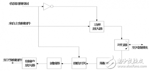
 A planar doped barrier layer (PDB) or Schottky diode in parallel with the transmission line. The limiter has low insertion loss and linearity at low input levels, providing protection against transient or short-term overload. In this paper, the series diode pair of HSMP2822 provided by Agilent is used as the limiter. Figure 3(a) shows the structure of the diode pair, (b) is the installation method of the limiter, and (c) is the limiter. Equivalent circuit diagram.
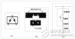
 Load to the ground. In order to meet the design requirements, two ADG901 series are used to improve the isolation. The insertion loss of the single-chip ADG901 has an insertion loss of about 0.5 dB in the frequency band in which the system operates, and the insertion loss of the two-piece series has about 1 dB. The isolation of the actual fabrication of the receiving switch is related to the characteristics of the chip, as well as the size of the wiring and shielding cavity. The measured isolation of the receiving switch made by two ADG901 series is 73dB, and the insertion loss is 1.1dB, which meets the design requirements. Figure 4 is a physical diagram of the receiving switch and limiter.
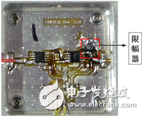
Design and Analysis of T/R Component of P-Band Transient Polarization Radar System
1 Introduction