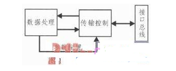
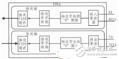
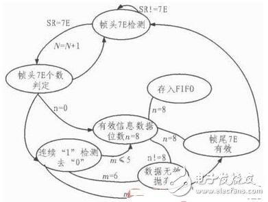
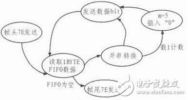
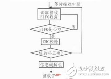
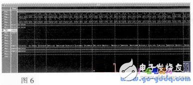
Aiming at the communication requirements based on HDLC protocol in the flight control analog device, a new FPGA-ARM based HDLC protocol controller design was completed. Firstly, the frame structure and cyclic redundancy check (CRC) principle of HDLC protocol are introduced. Then, combined with FPGA, the advantages of arbitrary data width operation and ARM programming are simple and flexible, and the frame structure and CRC of HDLC protocol are effectively realized. The application method meets the requirements of the HDLC protocol. The application results show that the design can meet the technical requirements of various functional indicators. High-Level Data Control (HDLC) is a synchronous data transmission, bit-oriented data link layer protocol with powerful, efficient and synchronous transmission of error detection. Currently HDLC protocol has become a communication. One of the most widely used protocols in the field is often used as a communication protocol for communication between flight control and steering gear, boosters, etc. in the field of aircraft design. The flight control simulation device is used in the development stage of the aircraft for flight control system software development and simulation evaluation. The flight control software is often A-level software, and any problem will cause flight failure, which will cause the whole system to be paralyzed. The software control algorithm is verified by the aircraft control system simulation device, and the software debugging and system verification of each subsystem can speed up the design progress of the aircraft and reduce the design risk and cost. The HDLC protocol controller studied in this paper is used for communication between the flight control simulation device of a certain type of aircraft and the steering gear controller. In general, the HDLC protocol is mainly implemented by using a dedicated chip and software programming. At present, there are many dedicated HDLC protocol processing chips on the market such as MT8952B and MK5025. These chips are reliable but highly functional and suitable for high-volume products for specific purposes. Software programming is done by programming for a microcontroller or signal processor, but since the microcontroller or signal processor is based on byte (8-bit, 16-bit, etc.) processing, the resolution and generation of HDLC protocol frames is geared toward The processing of bits, and thus this method greatly increases the load on the microprocessor or signal processor. Considering that there are a large number of different bus interfaces to be processed in the flight control simulation device in this design, the processor is FPGA+ARM, and the FPGA can process signals of any data width. ARM has the advantages of simple programming and flexible modification. Based on this, this paper uses FPGA+AHM to complete the data transmission control conforming to HDLC protocol. ARM completes the CRC checksum and unpacks the information frame, and finally realizes the design of HDLC protocol controller. HDLC is an advanced link layer control protocol, a bit-oriented data link layer protocol. HDLC is usually a point-by-point or point-to-multipoint structure. It can be used for half-duplex or full-duplex communication. It uses synchronous transmission and is often used in medium and high-speed data transmission. HDLC adopts the sliding window protocol, which can confirm several frames at the same time. In addition, each frame contains address locations, so in the multi-point structure, the primary station can establish connections with multiple slaves at the same time, and each slave station only receives the content. The frame of the station address, so HDLC transmission efficiency is relatively high, with a high throughput rate. In the HDLC protocol controller, the key to its implementation lies in two aspects. On the one hand, to ensure the uniqueness of the frame interval flag, the "0" bit insertion/deletion technique is adopted in the subsequent fields. When transmitting, all information except the frame interval flag is automatically inserted with a “0†as long as five consecutive “1â€s appear; similarly, the receiver receives five consecutive “1â€s when receiving data. Then automatically delete the following "0"; on the other hand, the CRC code is generated and verified, that is, at the transmitting end, the CRC is automatically generated by using the generator polynomial and attached to the information segment and sent out. At the receiving end, the received one frame data is checked by the CRC code. The full name of the CRC is Cvclic Redundancy Chcck, and the Chinese name is cyclic redundancy check. It is an important class of linear block codes. The coding and decoding methods are simple, have strong error detection and error correction capabilities, and are widely used in communication fields to implement error control. The basic principle is: for a given (N, K) code (after splicing the R-bit check code after the K-bit information code, N=R+K), it can be proved that there is a highest power NK=R Polynomial C(x). According to C(x), a check code of K-bit information can be generated, and G(x) is called a generator polynomial of this CRC code. The specific generation process of the check code is as follows: suppose the information to be transmitted is represented by a polynomial C(X), and C(x) is shifted to the left by R bits (which can be expressed as C(x)*2R), so that the right side of C(x) The R bit will be vacated, which is the position of the check code. The remainder obtained by dividing C(x)*2R by the generator polynomial G(x) is the check code. According to different R, a variety of different CRC standards are formed, such as (3RC-4: x4+x+1, CRC-8: x8+x6+X4+x3+X2+ X1, CRC16-CCITT: x16+X12+x5+ 1 etc. This article uses the CRC16-CCITT standard. 2.1 HDLC protocol processing circuit design In order to meet the requirements of aircraft design verification, flexible configuration based on HDLC protocol transmission can be realized. Its functions and technical requirements are as follows: 422 full duplex; adjustable transmission rate, up to 2 Mbps; communication distance not exceeding 5 m; communication error The rate is less than 10-7; the number of frame headers 7E and the end of the frame is adjustable, and the CRC check mode adopts CCITT-CRC16. According to the function and technical specifications and the overall configuration of the flight control analog device, the overall block diagram of the controller is shown in Figure 1. . Figure 1 Controller overall block diagram The data processing unit is implemented by ARM, completes the CRC check and information extraction of the data frame, and initializes the parameters of the transmission control unit according to the setting, including the baud rate, the effective number of 7E; the transmission control unit is implemented by FPCA, and the main function is Realize HDLC transmission control logic and data buffer; interface bus adopts full-duplex RS422 data bus. Because RS422 transmission line is differential voltage, level conversion is needed. For this reason, the controller designed in this paper selects MAX3491 as electronic conversion chip according to design requirements. Its conversion speed reaches 10Mbps to meet the needs. The paper will focus on the data processing unit and output control logic for the HDLC controller design. 2.2 HDLC transmission control unit HDLC transmission is bit-wise operation, so it is completed by FPGA. The FPGA adopts tera/'target='_blank'>Altera's CYCLONEII series FPGA. The development platform is based on QuartuslI 6.0 development environment, and the finite state machine design is used to realize HDLC protocol transmission control. Partly, and finally, the design implementation is given in the form of an IP core, which is convenient for developers to maintain and upgrade. Since the HDLC protocol controller is full-duplex communication, that is, the receiving circuit design including the HDLC sync bit data and the transmitting circuit design of the HDLC sync bit data frame. In the design of FPGA, both the receiving end and the transmitting end are bit-based processing, and its functional block diagram is shown in Figure 2. Figure 2 HDLC protocol controller transmission acceptance function block diagram At the receiving end, the data is always received according to the rising edge of the receiving clock RCLK signal. Before the information frame is sent, the frame header "7E" is judged, and the number of "7E" is recorded. When the number of "7E" meets the setting requirement, the start is started. The reception of the information frame, and the number 1 counter is turned on. When five consecutive "1"s are encountered, the subsequent "0" is deleted, and the serial-to-parallel conversion is performed at the same time, and the data is composed of 8 bytes into one byte and stored in the FIFO. After the byte is received, if “7E†is received, it indicates that the information frame ends, and the number of “7E†is recorded. When the number of “7E†meets the end of frame setting, it indicates that the frame is received, otherwise it indicates that the error is received. , discard the frame. Figure 3 is a state diagram of the received frame state transition. Figure 3 Accept frame state transition diagram At the transmitting end, after receiving the ARM start transmission instruction, the corresponding number of frame headers 0x7E are sent, and then the data is taken out from the transmission FIFO, and the parallel-to-serial conversion is performed, and the data is transmitted bit by bit to the Tx according to the falling edge of the set clock TCLK. On the line, and after continuously transmitting 5 bits "1", the bit "0" is automatically inserted, and after the end of the transmission, the corresponding number of frames 0x7E is transmitted, and the transmission is ended. The transmission frame state transition diagram is shown in Figure 4. Figure 4 transmission frame state transition diagram Figure 5 HDLC data processing unit data acceptance flow chart 2.3 HDLC data processing unit The HDLC data processing unit mainly completes the CRC check and packet unpacking task of the information frame, and the processing chip adopts the STM32F103 series ARM chip of STMicroelectronics, and the chip has the advantages of simple and flexible development and low cost. The processing of the data by the data processing unit also includes receiving and transmitting two parts, and receiving is taken as an example. The specific working flow chart is shown in FIG. 5. When entering the receiving interrupt process, the empty receiving FIFO is first read, wherein the last two read data is the CRC check code of the frame information, and the check code is used for CRC check, and the check adopts the CRC-16-CCITT standard. The value of r is 16 and the generator polynomial is: C(x)=x16+x12+x2+1 The traditional CRC check is to process the message bit by bit. For ARM, the efficiency is very low. In order to improve time efficiency, the usual idea is to change space by time. Considering that the inner loop is only related to the current message byte and the low byte of crc_reg, the corresponding CRC check code is queried for the crc_reg low byte creation number table, and the final loop is completed. If no error occurs, the result should be zero. The sending unit is similar to the receiving unit. For its inverse process, the information is first packed in the agreed frame format, then the CRC check is performed, the check code is placed in the last 2 bytes of the information frame, and the information frame is passed through the data bus. Stored in the transmit FIFO of the FPGA, and finally write the transmit flag, and start the FPGA to send the transfer control logic. To complete the design, ModelSim is first used for simulation verification. As shown in Figure 6, the ARM and FPCA read and write timings are generated by the stimulus file. A set of data conforming to the HDLC frame format is written into the FPGA transmit FIFO, and the transmission is initiated. The file shorts RX/RCLK and TX/TCLK to form a loopback. The FPGA receives the data according to the protocol controller and stores the data in the receive FIFO to complete the verification. Its logic timing satisfies the HDLC protocol frame format and communication timing requirements. Finally, according to the design requirements, the designed HDLC communication protocol controller is loaded onto the FPGA and ARM, and the loopback test is performed with the serial communication card BST23109. The card can realize the serial port synchronization mode, and the communication meets the requirements of the HDLC protocol. The test results show that the baud rate can reach 2 Mb/s and the bit error rate is 10-8 within 5 m communication distance. In this paper, the design of HDLC protocol controller is carried out for the application requirements of HDLC protocol in flight simulation device. The content of HDLC protocol is introduced firstly. Then the software and hardware implementation of HDLC protocol controller is introduced, which is given in detail in HDLC protocol controller. The implementation process is not counted. Through simulation and actual test, the baud rate is up to 2Mb/s and the bit error rate is 10-8 within 5m communication distance. During the delivery of the flight simulator, the controller is fully functional and can meet the technical requirements of each indicator. Capillary Tube Manometer Pressure Gaug,Capillary Tube Manometer Pressure Gauge,Plastic Pipe Manometer,Capillary Tube ZHOUSHAN JIAERLING METER CO.,LTD , https://www.zsjrlmeter.com