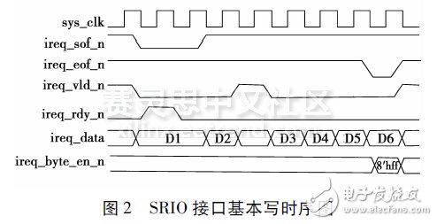
Abstract: Based on the analysis of data interaction in TImedivision-longtermevoluTIon (TD-LTE) RF conformance test system, in order to meet the large-capacity data interaction between field programmable gate arrays (FPGAs), design A high-speed embedded technology serial high-speed input and output port (serialrapidIO, SRIO), to achieve interconnection between two FPGA chips, to ensure the independence and interaction of upstream and downstream data processing in the TD-LTE system. Based on Xilinx's Virtex-6 series XC6VLX475T chip, the overall design scheme of SRIO interface is given. After ModelSim software simulation, the format type and transaction type of data interaction suitable for the project are determined, and the interface code is integrated and board-level verified. Online debugging, etc., compare and analyze the correctness of data transmission on the ChipScope software, compare the bit error rate of the transmitted and received signals through the test module, determine the stability and reliability of the SRIO interface in high-speed data transmission, and successfully verify the SRIO. The interface interconnects data between FPGAs, and the solution is applied to the development of TD-LTE RF conformance tester system as a new bus technology. With the continuous deepening of research on mobile communication technology, 3GPP LTE has gradually become an important mobile communication system supporting the world telecommunication service. In the research of time-division long-term evolution (TImedivision-longtermevoluTIon, TD-LTE) system, the application of various innovative technologies such as frequency division multiple access technology and multiple input multiple output (MIMO) technology [1] makes the processing power of the system More and more demanding, high-speed digital signal processing (DSP) and large-scale field-programmable gate array (FPGA) are widely used [2], relying only on improving the performance of single-processor to improve processing power The harder it is, the more real-time parallel processing technology must be used. Parallel processing of multi-processing chips is an effective solution to meet the processing power requirements of the system. Therefore, interconnection between chips is particularly important. The traditional hierarchical shared bus bandwidth and rate are very low, and its performance has reached the limit, which cannot meet the high-speed processing requirements of TD-LTE. Traditional parallel bus interconnects require a large number of pins, which introduces some problems in device packaging, testing, and soldering, and increases the complexity of application in the system. The serial high-speed input/output port (se-rialrapidIO, SRIO) interface has the advantages of fast speed, small number of pins, low system cost, and point-to-point or point-to-multipoint communication. The SRIO interface has been successfully applied to data interconnection between multiple DSP processing chips [3]. In the TD-LTE system with multi-FPGA processing chip system architecture, a new high-speed interconnect interface is urgently needed for baseband processing information interaction. After in-depth study of SRIO protocol [4] and related technologies, this paper designs a reliable open interconnect protocol standard, realizes the data interaction scheme between two FPGA chips, improves the data interaction capability, and improves the data interaction capability. The transmission delay is analyzed to meet the performance requirements of the TD-LTE radio frequency conformance test system. 1.1 Introduction to SRIO The RapidIOv2.1 specification released in May 2011 provides two interface modes (1x and 4x) [5], 1x uses less logic resources, and data bandwidth is lower; 4x requires more logic resources, but provides Higher bandwidth and better reliability. The clock uses an internal differential clock. The supported baud rate [6] is 1.25, 2.5, 3.125 and 5Gboud, respectively, to meet different application requirements. It also supports multiple transaction types, including read/write non-sharing. Registers, stream writes, maintenance, doorbells, and mailbox services. 1.2 SRIO Specification 1 logical layer. A variety of specifications are defined, including I/O logical operations, messaging, shared storage, flow control, and data flow, as well as the full protocol and package format of the interface. They provide the necessary information for the endpoint device to initiate and complete things. 2 transport layer. Defines the address space of RapidIO and provides the routing information required for packets to be transmitted between endpoint devices. 3 physical layers. At the bottom of the entire hierarchy, the details of the device-level interface are defined, specifying the packet transfer mechanism, flow control, electrical characteristics, and low-level error management [7]. 1.3 SRIO interface write timing According to the timing diagram generated by the FPGA client transmitting data through the SRIO interface [6], the basic timing diagram of the interface is shown in Figure 2. In Figure 2, sys_clk is the system clock, which is obtained by the input differential clock through the clock module, which is more stable than the ordinary single-ended clock; ireq_sof_n is the start signal, marking the beginning of a data frame; ireq_eof_n is the end signal, a data frame The end flag; ireq_vld_n is a valid signal, the data transmitted when the signal is low is valid; ireq_rdy_n is the start flag; ireq_byte_en_n is the bit enable signal of the data, and the lower 8 bits of ireq_byte_en_n corresponding to the data D6 in Fig. 2 are high, meaning The lower 8 bits of D6 are not enabled, and many other format control signals are not listed here. The SRIO interface acts as a data interaction channel between FPGAs. The data is transferred from the host to the slave through the interface and from the slave to the host. The FPGA is implemented by six main modules: interface control, clock, reset control, logic. Core, physical core, cache control. The following describes the internal implementation of the system and the functions of each module and the Veriolg language [8] implementation method [9]. In order to make the display of the simulation and implementation diagrams intuitive and convenient, the loopback method is used to demonstrate that the sending and receiving are the same host, and the destination address is the same as the source address. The interface control module is the start and end of the entire system, through which the user can control the size, type and format of the required interaction data. Random access memory (RAM) is a relay station used by the FPGA to transmit data. The data exchange function between the two FPGA chips is realized by controlling the data in the RAM. SRIO uses a dedicated differential clock with a frequency of 156.25MHz or 125MHz. Different clocks have different transmission rates. The user of the differential clock is NET "sys_clkn" LOC=“G9â€; NET “sys_clkp†LOC=†G10". Here, the differential clock is first passed through the differential clock buffer (IBUFDS_GTXE1) and the clock division management unit (MMCM_ADV) to obtain two clocks UCLK and UCLK_DV4, which are used to drive other modules. 2.1 FPGA design hardware environment 2.2 FPGA internal implementation scheme block diagram According to the principle of SRIO interface constitutes the system, the SRIO interface hardware implementation principle block diagram can be designed, as shown in Figure 3. SRIO completes the data interaction between two FPGA chips, and the two parts of the schematic are symmetric. The logical layer interface consists of three parts: user interface, link interface, and maintenance interface. The user interface is composed of four signal ports, which are the initial request ireq, the initial response iresp, the target request treq, and the target response tresp. The user can configure the four signal ports through the interface control module to implement data remote or write operations. The link interface is used to communicate with the physical layer and the data exchange of the buffer. Maintenance operations can be used to send certain information, such as error indicators or status information for devices that do not have endpoints. The data payload is usually placed in the queue of the target endpoint and generates an interrupt to the local processor. The buffer balances the balance between system performance and resource usage, and the size of the buffer interval for sending and receiving is configurable. The cache core can handle all packets returned from the physical layer, including packet retransmissions and error recovery. It ensures that the packet arrives correctly at the receiving end and at the physical layer. The physical layer core (PHY) handles link adjustment, initialization, and protocol, including the insertion of a cyclical redundancy check (CRC). Finally, a data collection module is added to the interface control module to collect valid transmit data ireq_data and receive data treq_data, and then compare the error rate with matlab software. Residual Current Circuit Breaker With Over Load Protection
TWO FUNCTION : MCB AND RCCB FUNCTIONS
leakage breaker is suitable for the leakage protection of the line of AC 50/60Hz, rated voltage single phase 240V, rated current up to 63A. When there is human electricity shock or if the leakage current of the line exceeds the prescribed value, it will automatically cut off the power within 0.1s to protect human safety and prevent the accident due to the current leakage.
RCBO,ELCB,Leakage Circuit Breaker,Residual Current Circuit Breaker,Residual Current Circuit Breaker with Over Load Protection 1p,Residual Current Circuit Breaker with Over Load Protection 2p Wenzhou Korlen Electric Appliances Co., Ltd. , https://www.korlen-electric.com
SRIO is a system internal interconnect technology for system internal interconnects of high-performance embedded devices and provides the scalability, robustness, and efficiency that embedded system developers require. RapidIO uses packet switching technology to provide high-speed, low-latency, stable and reliable interconnectivity between network processing units (NPUs), central processing units (CPUs) and DSPs. Possible applications include multiprocessors. Data interaction between memory mapped I/O devices, storage subsystems and general-purpose computing platforms in memory and network devices has broad application prospects.
SRIO uses a three-tier hierarchical architecture [4], as shown in Figure 1. 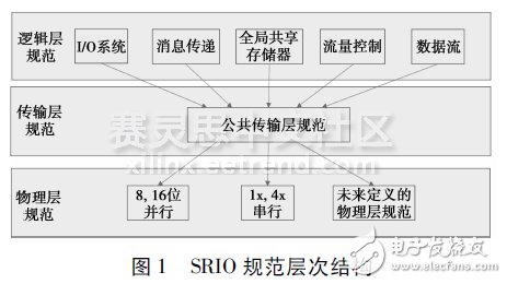
The FPGA is based on two Xilinx Virtex-6 series XC6VLX475T chips. Based on a 40nm manufacturing process using the third-generation Xilinx ASMBLTM architecture, the Virtex-6 FPGA family also features next-generation development tools and extensive IP library support already developed for the Virtex-5FP-GA. The Virtex-6 FPGA combines advanced hardware chip technology, innovative circuit design techniques, and architectural enhancements to deliver significantly lower power, higher performance, and lower cost than previous Virtex devices and competing FPGA products. 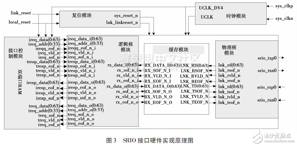
The reset module generates a reset signal for the entire project. Here, asynchronous reset synchronous release is used. When a system reset signal occurs, the module will issue a link reset signal.
) and confirm the identifier into the output packet. The PHY uses a dedicated 8B/10B code (ie K code) to manage the link, including flow control, packet delimitation, and error reporting.
leakage breaker can protect against overload and short-circuit. It can be used to protect the line from being overloaded and short-circuited as wellas infrequent changeover of the line in normal situation. It complies with standard of IEC/EN61009-1 and GB16917.1.