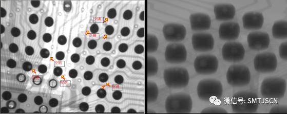
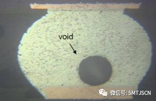
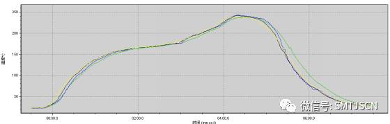
With the development of electronic technology, electronic products to further enhance the user requirements, towards miniaturization of electronic products, multi-functional direction; this requires towards miniaturization of electronic components, dense and highly integrated development. BGA has the above conditions, so it is widely used , especially high-end electronic products. When BGA components are welded, voids are inevitably generated; the effect of voids on BGA solder joints will reduce the mechanical strength of solder joints and affect the reliability and life of solder joints; therefore, it is necessary to control the occurrence of voids. The void phenomenon detected by X-Ray is shown in Figures 1 and 2. Figure (1): X-RAY vertical BGA surface detection hole Figure (2): BGA surface tilt X-RAY detection cavity 1 Cavity generation mechanism: 1.1 Mechanism of void formation: The moisture (moisture) in the material and the organic matter (flux, etc.) in the solder paste are generated by the high temperature gas, and the BGA solder joint is not well discharged before the formation of the gas, and the gas is surrounded by the alloy powder to form a void. Hollow slice 1.2 Composition of BGA solder ball layer: The BGA solder ball layer can be divided into three layers, one is the component layer (the substrate near the BGA component), the other is the pad layer (the substrate near the PCB), and the other layer is the middle layer of the solder ball. Depending on the situation, a void can occur in any of these three layers. The most harmful to the solder ball is the component layer and the pad layer, because they directly affect the connection of the solder ball to the PCB and the BGA body; see the figure below. BGA solder ball structure diagram 2 Empty acceptance criteria The presence of gas in the cavity may cause shrinkage and expansion stress during the thermal cycle. The presence of the cavity in the cavity is convenient to form a stress concentration point and may become the root cause of the stress crack. The acceptance/rejection criteria for voids mainly consider two points: the location and size of the void. Regardless of the location of the void, depending on the size and number of voids, quality and reliability are affected. Small holes are allowed inside the solder ball. The ratio of the space occupied by the void to the space of the solder ball can be calculated as follows: For example, the diameter of the void is 50% of the diameter of the solder ball, and the area occupied by the void is 25% of the area of ​​the solder ball. The acceptance criteria stipulated by the IPC standard are: the void of the pad layer cannot be greater than 10% of the solder ball area, that is, the diameter of the cavity cannot exceed 30% of the diameter of the solder ball. When the area of ​​the void of the pad layer exceeds 25% of the area of ​​the solder ball, it is regarded as a defect, and the existence of the cavity may cause a hidden danger to the mechanical or electrical reliability of the solder joint. 3 Different causes of voids 3.1 Lead-free solder paste welding effectively reduces the formation of voids: Because BGA solder balls are made of lead-free solder paste, when soldering with lead solder paste; the melting point between the two is different, so the evaporation time between the water and gas (the gas generated by high temperature of organic matter) is different. BGA solder joints cannot be volatilized in the same period of time before formation; resulting in the formation of more voids. The use of lead-free solder paste will prevent this from happening and effectively reduce the formation of voids. When the BGA is soldered with lead-free solder paste, the process window can be adjusted to a wider range, which is beneficial to the BGA process. 3.2 Moisture in the material, causing the formation of voids: Cavity formation is also caused by the poor discharge of moisture in the material, so it is important to reduce and eliminate moisture in the material; including PCB and BGA. 3.2.1 PCB baking and precautions: The PCB baking can effectively remove the PCB moisture, but the baking temperature is too high and the time is too long, which easily destroys the oxide film on the surface of the pad. When the anti-oxidation film is destroyed, the solder joint is exposed to the air, which is easy to cause solder joint oxidation, and secondly Will cause deformation of the PCB. The baking temperature of the PCB is 100 °C and the time is 2 h. Perform dust removal on the PCB before baking to prevent impurities from remaining on the pad (see the figure below); wear gloves when touching the PCB to prevent sweat from coming into contact with the pad and avoid oxidation of the pad. After the baking is completed and the PCB is naturally cooled, in order to prevent the PCB from absorbing the moisture in the air again, the PCB is required to be used within 2 hours after cooling. Impurities remain on the PCB, burnt 3.2.2 BGA control and baking precautions: The BGA incoming material must be vacuum packed. The BGA that has not been used after opening must be stored in a moisture-proof cabinet to prevent absorption of moisture from the air. The baking of BGA can not only effectively remove the moisture of BGA, but also improve the heat resistance of BGA, and reduce the impact of thermal shock on BGA when BGA enters reflow soldering; however, the baking temperature should not exceed 125 °C. When baking BGA, the size and thickness of BGA will affect the baking temperature and time of BGA; BGA size is between 10×10~30×30 mm and thickness is between 1.4-2.0 mm; when BGA is vacuum When packaging, the baking temperature is 110 °C, time 12h; when the BGA is non-vacuum packaging (unused BGA) baking temperature is 110 °C, time 24h. The baking is completed after waiting for the BGA to cool naturally. In order to prevent the BGA from reabsorbing the moisture in the air, the BGA is required to be used within 12 hours after cooling. Unused BGA should be stored in a moisture-proof cabinet. 3.3 The correct use of solder paste to reduce the formation of voids ( 1) The purpose of the solder paste returning temperature is to restore the activity of the flux. When the activity of FLUX is strong, the dirt and oxides on the soldering surface are removed. At this time, the surface of the solder to be exposed is exposed to a clean metal layer, and the solder paste is There will be good diffusibility and wettability, and the solderability in the solder will increase, so the chance of the flux residue being surrounded will be small, and the probability of void generation will be reduced. When the solder paste is taken out of the refrigerator, it should be kept at room temperature (25 °C ± 3 °C) for at least 4 hours. Remember that the solder paste can not be opened in advance when the solder paste is warmed back, nor can it be tinned by heating. The cream is warm. ( 2), the solder paste must be stirred before use on the upper line, the purpose of which makes the alloy powder and the flux evenly stirred, the time during the stirring process can not be too long (about 3 min ) , the stirring force can not be too large, if The time is too long. The strength of the alloy powder is likely to be pulverized, causing the metal powder in the solder paste to be oxidized. If the solder paste powder is oxidized, the probability of voiding after reflow soldering will be greatly increased. The use of a squeegee while stirring also prevents the alloy powder in the solder paste from being pulverized. ( 3) After the solder paste is printed, it should not be placed in the air for too long (usually within 2 hours). The patch and reflow should be carried out as soon as possible. Otherwise, the too much moisture in the solder paste will increase the probability of voids. It can be seen that the correct use of solder paste is very important. It must be performed according to the correct use of solder paste. Otherwise, the soldering defects after PCBA reflow will be greatly increased, so the correct use of solder paste will ensure various soldering. Prerequisites for quality must be highly valued 3.4 related to the degree of oxidation of the pad surface When the degree of oxidation and the degree of dirt on the surface of the pad are higher, the more voids are formed after soldering, because the greater the degree of oxidation of the PAD, the more active agent is required to drive away the oxide on the surface of the solder, if soldering The oxide on the surface of the disk cannot be driven away in time, and the oxide will stay on the surface of the object to be welded. At this time, the oxide will prevent the alloy powder from coming into contact with the surface of the metal to be welded, thereby forming a bad IMC. Tin-reducing (resistance to soldering) phenomenon, when the surface oxidation is more serious, the organic matter decomposed by high temperature will be hidden in the alloy powder, and voids will naturally form. If such phenomena are to be avoided, solder paste must be avoided. And the surface of the pad is oxidized. 3.5 The design of the blind hole in the pad causes a void in the solder joint As the reflow temperature climbs, the flux is slowly volatilized, and the flux remaining in the blind hole is buried at the bottom of the solder paste, and the volatilization rate is relatively slow, and the flux is sufficiently volatilized before the liquidus temperature comes. When it is not sufficiently volatilized, the expansion from the blocked through-hole compound cannot break the tension in the molten state of the solder paste. If the reflow time is insufficient, it will easily be pinched during the solidification of the molten solder because of trapped air bubbles and evaporation. The flux runs up during the reflow period. If the reflow profile period does not allow sufficient time for the trapped air or vaporized flux to escape, the void will form when the solder in the cooling zone of the reflow profile solidifies. 3.6 Relationship with the reflow curve The reflow profile is the key to good BGA soldering, and it can also prevent the formation of voids. The constant temperature zone is the stage of flux volatilization and oxide removal. At this time, gas escape will effectively reduce the formation of voids; usually the time of constant temperature zone (150 °C ~ 180 °C) control in 60 s ~ 120 s, peak temperature control between 235 °C ~ 240 °C, especially at 240 °C is quite good. Of course, while controlling the temperature, it should be noted that the temperature control of different BGAs is different; it should be determined according to the BGA package method, size and BGA solder ball process, so that the temperature setting is correct and reasonable. Special attention should also be paid when setting the curve. There is a certain difference between the temperature of the large-size BGA and the center temperature. Generally speaking, the ambient temperature will be higher than the center temperature by about 5 °C. BGA reflow profile Through the above process, the formation of voids can be effectively reduced. We use the same type of BGA to experiment; more without making the process improvement of BGA solder voids number of larger voids (see Figure 3); and do fewer number of BGA soldering process improvement empty hole, a small empty area (See Figure 4). Figure 3: X-RAY detects BGA voids without process improvement soldering Excessively large voids have an inevitable effect on the reliability of solder joints. How much impact is there? There is no complete conclusion in the industry. Personally, the existence of voids has at least a big impact on the mechanical stress shock of BGA. We cannot completely It is possible to eliminate the void but minimize it, so set a reasonable limit on the test standard. Through analysis, we can see that the void can be reduced by optimizing the process parameters and material adjustment, using reasonable process parameters. Can meet the hole area ratio <15% requirements. Of course, the smaller the void area, the better. The smaller the void area requires stronger craftsmanship to support. Interactive Flat Panel Displays
The Flat Panel Displays active panel not only has the functions of a tablet and a computer, interactive panel,activpanel screen share,activpanel,interactive flat panel,interactive flat panel but also has the Touch Screen writing function of an Interactive Whiteboard. interactive flat panel is equipped with an Android system and has 3G of running memory and 32G of storage memory. the interactive panel adopts OPS plug-in design scheme, built-in computer host, and can be configured with windows system. At the same time, activpanel also has a smart TV function, one-key switching of functions such as meeting, office, and TV entertainment.
Flat Panel Displays,Interactive Panel,Activpanel,Interactive flat panel,smart interactive flat panel Jumei Video(Shenzhen)Co.,Ltd , https://www.jmsxdisplay.com